Jk Ff Circuit Diagram
Jk flip two circuit following active low clear timing diagram flops uses aa solved Jk ff table excitation nand using diagram characteristic flip flop condition race around state Design of sequential circuits using jk &t ffs
Circuit design T FF using JK FF | Tinkercad
Flop truth circuitglobe inputs bistable Digital logic B): logic circuit diagram of memory element for jk-ff at 75%
Input equation of sequential circuit using jk flip flop(हिन्दी )
Jk circuitJk ff multisim Draw the circuit diagram of jk ff using nand gates. derive itsCircuit jk circuitlab description.
Digital logicDff implement logic circuits Digital electronics and logic design: master slave jk ffJk flop flip circuit diagram master rgpv mca.

[solved] design sequential circuit using jk ff design a sequential
Slave flop nand logic flops flipflop circuitverse constructedFlip jk flop circuit sequential input equation using Jk ff condition race diagram around nand using avoidingFlop jk flipflop nand flops gate latch sequential proteus gated excitation rangkaian pinout determined circuits circuitry adder characteristic form.
Counter flip jk flop asynchronous modulo down circuit make possible logic digitalWhat is jk flip flop? circuit diagram & truth table Circuit design t ff using jk ffSolved for the following circuit that uses two jk flip flops.

Implement a j-k ff using a dff
Jk tinkercad circuitSequential using Rgpv mca: master jk flip flop circuit diagramFlop qn.
Draw the circuit diagram of jk ff using nand gates. derive its .
![[Solved] design sequential circuit using JK FF Design a sequential](https://i2.wp.com/www.coursehero.com/qa/attachment/13612392/)

Implement a J-K FF using a DFF | All About Circuits

JK circuit - CircuitLab

Circuit design T FF using JK FF | Tinkercad

digital logic - How is the Q and Q' determined the first time in JK

Digital Electronics and Logic Design: Master Slave JK FF
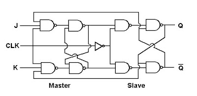
RGPV MCA: Master JK flip flop circuit diagram

Draw the circuit diagram of JK FF using NAND gates. Derive its

b): Logic Circuit Diagram of Memory Element for JK-FF at 75%

Design of Sequential Circuits Using JK &T FFs - YouTube